IDT8T79S818I-08
IDT8T79S818I-08 is 1-to-8 Differential to Universal Output Clock Divider/Fanout Buffer manufactured by Integrated Device Technology.
1-to-8 Differential to Universal Output Clock Divider/Fanout Buffer
General Description
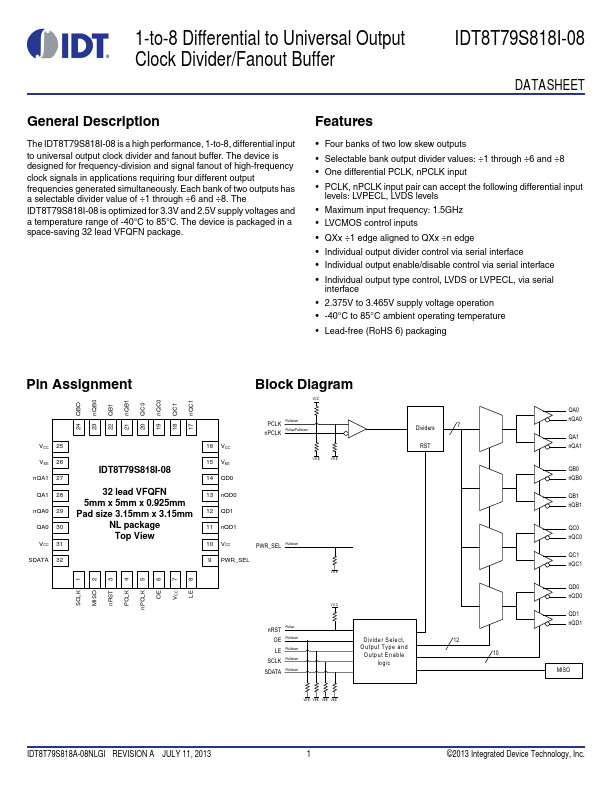
The IDT8T79S818I-08 is a high performance, 1-to-8, differential input to universal output clock divider and fanout buffer. The device is designed for frequency-division and signal fanout of high-frequency clock signals in applications requiring four different output frequencies generated simultaneously. Each bank of two outputs has a selectable divider value of ÷1 through ÷6 and ÷8. The IDT8T79S818I-08 is optimized for 3.3V and 2.5V supply voltages and a temperature range of -40°C to 85°C. The device is packaged in a space-saving 32 lead VFQFN package.
Features
- Four banks...